![]()
1998 Winter IEEE/PES
STS Panel Session Paper
STS Design Requirements &
Considerations
by
Colin E.J. Bowler, ABB - US
Power Systems Inc.
Introduction
Much has been written about the STS
application relative to requirements and value, however, very little has been
written or said about what is required to achieve a workable STS, considering
the following important areas of design:
- Control Signal Measurement
- Non-Sinusoidal Load Current Operation
- Transfer Operation
- Up-Stream/ Down-Stream Fault Discrimination
- Protection Functions
- Monitoring Functions
- Cooling Methods
- Main Circuit Design.
These areas concern some important
specification requirements that are not easily met, and require a control
capability far in excess of the more common voltage control devices such as the
SVC. Establishing and meeting these requirements is the subject matter of this
paper.
The most important reason for the complexity
of control is the fact that the STS is applied in series with the power
system elements, using a discontinuous switching device like a thyristor, and
to create from it a behavior similar to a perfect conductor in the on-state,
and a high impedance off-state. Because the STS is in series with the load, the
STS must be able to perform these functions for arbitrary current level,
current shape, and power-factor; from load-transformer low load pick-up, and up
to full short circuit current, without introducing any appreciable current or
voltage discontinuity of its own making, such as might be caused by delayed
gate signal application. These facts lead us to the following discussions.
Control Signal Measurement
As a power system controlled device, the STS
is required to measure its applied voltages and currents, act on the embedded
information in these signals and exercise control of a thyristor switch as
determined by its control functions, and also respond to operator inputs.
The most demanding requirement for
measurement is the dynamic range of current that must be measured. In the case
of cold load pick-up the load current may only be a few amperes such as for a
power transformer excitation current, or just feeder capacitive reactive
loading. In the case of short circuit operation the current may be hundreds of
thousands of amperes. For a typical 15 kV feeder we may see a range of 50,000
:1 for instantaneous current level maxima.
Under this range of current conditions the
control is required to track current zero points to affect thyristor switching
current polarity reversal, at the identical instants as if the switch were
replaced by a normal conductor. The measurement requirements to deal with this
situation are very demanding because the signal-to-noise ratio is highly
variable unless special means are taken to control this factor. Noise in the
analog signal is inevitable, especially because of the need to isolate the
signal source galvanically, to meet surge requirements, and to isolate high
common-mode voltages from the control electronics. This noise source generally
precludes using a high order (16 bit) converter to full advantage, because if
we set gains for low level signals, the high level signals will be clipped
(distorted) and this is not allowed (see below); while if we set-up the
measurement for distortion-free high-current measurements, the noise will
approach the signal level at low current, and consequently current zero
switching will not be possible (also required, see below).
One method to achieve the required
signal-to-noise over the wide range of operating currents is to use automatic
gain control of the signal ahead of the signal isolation device. One approach
would use two digital control bits for a gain controlled instrumentation
amplifier to achieve four input gain settings (e.g. 1, 10, 100, 1000) that are
automatically switched by the control according to the instantaneous current
level being measured. The control is in charge of the gain settings and
obviously knows the effective gain to use in calibrating the signal information
to actual engineering significance for use in the firing control algorithm.
Even with this programmable gain amplifier (PGA) capability, it is still useful
to utilize a wide range 16 bit analog-to-digital converter in order to deal
with the remaining range of signal-to-noise at each gain setting, and to reduce
internally generated noise, such as quantization, and a host of other sampling
induced noise effects.
The second important measurement requirement
is the need for minimum phase delay, input to output, so that firing signals
going to the thyristor switches are also not delayed. This requirement sets
conditions on the control algorithm for detecting current zeros, namely phase
compensation, which are affected by both the accuracy of signal measurement,
and the sample rate of data acquisition. Signal accuracy and sample rate are
tied together in a digital control because of signal aliasing, the creation of
in-band signals due to too low a sample rate. To avoid aliasing requires the
sample rate to exceed the bandwidth of the signal information by a wide margin
(typically 3:1 minimum). This sets the parameters of signal filtering in terms
of roll-off rate and bandwidth. A suitable data acquisition arrangement that
meets these requirements would have an 8 pole linear phase anti-aliasing
filter, sampling at 120 samples per power frequency cycle. Linear phase
filtering is a requirement to eliminate signal distortion, and to allow simple
digital correction of phase delay in the firing control, even under transient
conditions. With these measurement provisions, it is reasonable to proceed with
firing control design requirements evaluation.
Non-Sinusoidal Load
Current Operation (Firing Control)
Firing control of a thyristor switch at
prospective current zeros points, is well understood for situations when the
currents are near sinusoids, such as for SVC type equipment. The SVC is a shunt
connected device that is of known impedance, where the voltage applied varies
over a small range. In contrast, the STS is series connected and the impedance
of the load is always unknown. What is required for firing control generally,
is a synchronous phase-locked sample data collection system that tracks the
system frequency variations. One approach for this will sample voltage and
currents synchronously based on phase-locking the sampler to a system voltage,
using a digital phase-locked loop (PLL) control algorithm. The computation of
the time to current zero, the firing point of the next thyristor switching, is
determined from a phasor calculation of the individual phase voltage and
current sinusoids relative to the phase-locked reference signal.
In the case of an STS, the control has no
information about the load current expectation, other than it can be almost
arbitrary in level and harmonic content, and will generally exhibit transient
phenomena on odd occasions, including long-term dc-offsets (transformer inrush
current). Tracking current zeros in this environment is very difficult, but is
required of the STS if the control is to avoid introducing changes in the
current due to firing activity. To do otherwise will create chaos of the load
voltage and as a result produce power quality problems rather than eliminating
them.
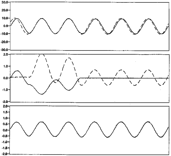
|
|
Bus Voltage |
|
Line Current |
|
|
Firing pulse + |
|
|
Firing pulse - |
|
|
Mode Selector |
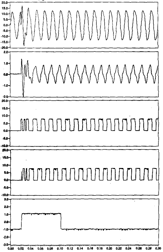
Figure
1, Firing Mode Tracking Control
It is possible to track current zeros for
arbitrary current shapes with time, by special interpolation algorithms that
can be executed in modern digital signal processor type cpu’s, in real-time.
Such a control is illustrated in Figure 1, demonstrating a three mode control,
for tracking changes in transient, harmonic, and harmonic free sinusoids. Mode
changing is seen to be almost instantaneous with the change in the signal
quality as illustrated by the firing point tracking of the current zeros, and
the mode predictor output.
Transfer Operation and Up-Stream/Down-Stream Fault
Discrimination
The objective of the STS is to switch
(transfer) the power to the load from a preferred source to an alternate source
automatically and rapidly when a reduced voltage (imperiling power quality at
the load) is established in the preferred source, and while the alternate
source meets certain quality criteria. Usually the need to transfer power
supplies is because of an up-stream fault that may reduce the preferred source
voltage transiently.
Two algorithms are required to pull this off
namely:
·
High speed fault
direction indication
·
High speed transfer
algorithm
In the case of the up-stream fault the
transfer operation must be accomplished rapidly in the faulted phase and in a
manner that does not transfer the fault to the alternate source even for a
fraction of time, as may happen if the transfer algorithm is not very
intelligent. Figure 2, indicates that for the condition shown, operating the
S2+ thyristor gate, on fault detection, at the instant when current would want
to flow in this direction from the preferred source will transfer the fault to
the preferred source until the next current zero of S1. The transfer algorithm
must then be intelligent enough to pick the right polarity of the alternate
source switch, relative to the preferred source current polarity, in order to
switch at the earliest instant in time to affect source commutation without
fault transfer, and at the same time minimizing voltage disturbance at the
load. The corollary situation is to prevent transfer during a down-stream fault
incident, because this would transfer the fault to an otherwise healthy feeder,
which is not too smart considering the additional number of customers that
would be affect by this act.
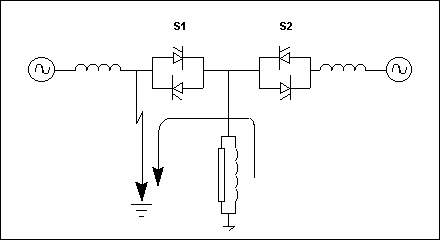
Figure
2, Avoidance of Fault Transfer
We note that the detection of the up-stream
fault, and the transfer action must be very fast in order to minimize power
quality issues. This means that the detection of a down-stream fault must be
equally fast in order to inhibit transfer. Ideally, the fault direction
detector and the transfer algorithm must be essentially instantaneous in order
for the transfer switch to operate in a sub-cycle time window.
These requirements represent a very tall
order for the control, compared with algorithms that are typically used for
this in modern digital protective relay applications, where at least a
half-cycle is used to make a determination of magnitude, and much longer is
required to determine phase information accurately. A relatively high sample
rate, and very intelligent signal processing make this possible in the STS
control.
The reason that an STS can operate in
sub-cycle time at all, using thyristor based switches, is based on their rapid
forced commutation resulting from the under-voltage on the preferred source,
and the much higher voltage on the alternate source forcing open the preferred
source thyristor. Figure 3, illustrates a typical forced commutation switching
operation. The expedient of transferring the gate signal at the correct
instant, allows the force commutation of the thyristor switch to take place
naturally. This kind of switching is called make-before-break switching,
because during the transfer, current flows briefly (recovery current) from the
alternate source to the commutating thyristor in the preferred source. For
phases in the switch that are not affected by low voltage, the transfer
switching is called break-before-make. This latter kind of switching is normal
commutation at the next available
|
|
Bus
Voltage |
|
Source
Current
|
|
|
Load Current |
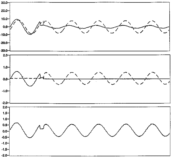
Figure 3, High Speed Transfer Operation
current zero after thyristor gate signals
have been removed. There may be a slight delay in this type commutation to
allow the control to be sure that current zero has been achieved in the
preferred source, prior to gating the alternate source. Manual switch operation
is also of the break-before-make variety.
Figure 4 illustrates an incorrect high speed
transfer that resulted in fault transfer. Here, the delayed fault current zero,
due to dc-current offset, also played a role causing the fault to be fed from
both sources for two cycles.
|
|
Bus Voltage |
|
Source Current |
|
|
Load Current |
Figure
4, Incorrect Transfer Operation
Monitoring & Protection Functions
It takes a very large number of power and
signal electronic components to construct an STS system. This is so, because
many identical power electronic devices are required in series to handle the
voltage, and parallel branches may also be required to handle the highest
current levels. As a consequence of this, there are many potential failure
modes that may cause switch malfunction. Actual failure modes are minimized by
careful component selection for reliability in the operating environment.
However, the control system must still provide for protection from equipment
failure to:
1. protect from producing power quality problems, and 2)
to protect the valuable equipment from additional failure.
An important quality in design of the STS
is self protection, i.e. fail-to-safe-condition, from any major failure in the
firing control computer, such as software error for example. While every effort
is made to make the software and hardware reliable, care is required in design
to allow the switch to turn-off naturally, as soon as practical, in the event
of failures of this type. This condition can be achieved, in this case, by
using a high sample rate for data collection, and requiring up-date of the
firing time every sample, so that if up-date does not occur due to some
failure, the timer will never re-fire the thyristor switch.
Because we are dealing with a thyristor
switch, many hardware failure modes may result in serious consequences for the
load current.
For instance a failure to gate a
thyristor on one switch polarity side, or a delay in firing will cause dc and
harmonics to be present in the load current and voltage, induced by this
failure. This leads to a requirement for harmonic and misfire protection to be
built into the control protection algorithms.
|
Protection Type |
Indication |
Action |
|
|
|
|
|
Unbalance Current |
Exceeds specification |
Transfer |
|
Over-temperature |
Excessive RMS current |
Turn on more fans or transfer or by-pass & trip |
|
Transient over-temperature |
Excessive peak current |
Transfer |
|
Misfire |
Protect load |
Transfer or Trip & by-pass |
|
Excess harmonics |
Higher than specification |
Transfer |
|
Over-voltage |
Greater than twice rated |
Transfer |
|
Gate Failure |
Stack stops conducting |
Transfer |
|
Thyristor failure |
More than 2 in one phase |
Transfer |
|
|
One failure in one phase |
Alarm |
|
Power Failure |
|
Alarm Bypass Trip |
Table
1, STS Protection Functions
The preferred list of protection
functions and actions is given in table I.
Many of the protection functions are
similar to those used in other electrical apparatus, the main differences
relate to the special considerations required in thyristor applications.
Excessive peak current is one of these, which relates to the local temperature
of the semi-conductor junction which has a short thermal time constant on the
order of milliseconds. The sensitivity here requires a thermal analog algorithm
executing in the control computer, to predict the temperature based on the
thyristor volt-ampere relationship including its variability with temperature.
Other protections in this category include loss of the gate signal, and the
protection from a shorted thyristor element.
Typically a thyristor switch for 15 kV
application may contain eight or so thyristor elements in series in order to
withstand the voltage applied when not conducting (blocked). Obviously the loss
of a gate signal to one level will cause an over-voltage on that level when the
other thyristor elements in series start conducting. The failure mode in this
case is likely a shorted thyristor. The gate failure monitoring provides a
rapid means of detecting this condition, for which the protection function can
operate and save the thyristor from total failure by transferring the switch to
the alternate source.
It is important to notice that the
transfer option for protective action, is utilizing the alternate source as a
means to maintain supply reliability to the load for internal switch failures
as well as for external event power quality issues. This is important, and is a
contrast with other competing power quality device mitigation solutions that do
not have this natural redundancy as part of the design, such as in the case of
an SVC or other voltage regulating device. This feature should be evaluated
carefully because it makes the STS intrinsically more reliable than some of its
competing alternatives.
Monitoring Functions
There are a number of monitoring
functions of value in the STS to provide inputs to the protection system for
the thyristor elements. These are:
·
Gate Reception
Detection
·
Heat Sink
Temperature Measurement
·
Thyristor Failure
Detection
These monitor functions occur on the high
voltage elements of the switch, and the information detected must be
communicated, via a galvanic isolation barrier, to the control for protective
action to take place.
Gate reception monitoring is important to
provide early warning of a failure of the control to deliver a switching
impulse to the gate of the thyristor. This function is both a protective system
input as well as a monitoring of the health of the switch. A failure to gate a
thyristor on time will assure its failure from over voltage. There are many
systems required to be working in order for the thyristor gate to be energized
including: analog signal measurement, the firing time computer, the pulse
output timers, the gate energy delivery system, and the gate information
delivery system. The gate reception monitoring system, working on every level
of the switch, together with the thyristor failure detection system and
thyristor temperature monitoring serves to narrow down the causes of thyristor
failure.
Thyristor temperature monitoring systems
are useful to protect the STS from cooling system malfunction, as well as to
protect from operation outside of the switch design specification. The
objective of the temperature monitoring system should be to predict the
temperature of the thyristor junction. This element of the switch is the
smallest in terms of thermal inertia, and is small enough to be affected by the
cycle by cycle values of peak current. The thermal analog energy storage vs
cooling temperature model must calculate the heat generation of the thyristor,
which is nonlinear with temperature, and the cooling effect of the heat sink
effects in the solution of the heat flow equation. Ultimately the switch can be
transferred to the alternate source in order to allow for cooling, but in worst
cases would provide a trip as the protective means for the complete series
thyristor string.
While the cause of thyristor failure is
required to be known, we also must detect the fact of the actual thyristor
failure when it occurs. Failure to detect will result in operation of the
switch with a higher voltage per thyristor level. Ultimately the number of
failures will increase until the string of thyristor element is too short to
support voltage, resulting in complete failure of all of the thyristor in the
series string. Detection of a single thyristor failure is then vital so that
maintenance of the thyristor string can be accomplished before such complete
failure occurs.
Cooling Methods
The type of an electrical apparatus is
indicated by its ability to work at its rating at the highest expected ambient
temperature. Thus the equipment rating is primarily controlled by the ability
to cool the apparatus. In the case of a thyristor based transfer switch we have
the option of air or water cooling based on existing technology. For
transmission equipment thyristor application (HVDC, SVC etc), water cooling has
generally been used to maximize equipment utilization to allow very high
ratings. Industrial applications of thyristor elements, such as drive systems,
have traditionally been air cooled. This is more for convenience, recognizing
the lower required equipment ratings and the ability to use air as an option.
The use of air cooling allows the choice of free or forced convection. Forced
convection provides for a more compact equipment as fans take up little space
while providing an order of magnitude increase in heat transfer capability.
A major consideration in air cooling,
especially for an outdoor or indoor electrical apparatus is the question of
audible noise. The control of noise begins with attention to pressure drop and
flow rate. The higher these figures the higher the potential noise induced by
flow buffeting. Once flow is established, acoustic noise may be amplified by
resonance with the mechanical structure.
Air cooled apparatus must also be
designed to handle air-borne pollution, especially particulate matter that may
block air passages over time. For outdoor application there is also the need to
consider moisture, which increases the collection of particulate matter in a
condensing atmosphere. One approach, to cater for outdoor switch application
with forced air cooling, is to provide separate internal and external air flows
using an air-to-air heat exchanger, or air-to-water heat exchanger. This
arrangement allows the internal air to be maintained none condensing by the
expedient of heating the air above the dew point of the internal air. Under
normal loading there is enough local heat to perform this function. For the
occasions when current is low, and with low ambient temperature, heaters may be
employed in the internal air path to stay in the non-condensing region.
The use of forced air cooling allows the
possibility of regulating temperature by fan control. Where dual redundant fans
are available, each may be operated separately, so that in cold weather no fans
will run. As ambient temperature increases, the single fan will regulate an
acceptable temperature for operation up to a 40oC ambient. For
extreme conditions or if for some reason air flow is impeded, the second set of
redundant fans will be called into operation to maintain temperature to
acceptable limits. Above some maximum operating temperature the switch may be
tripped to protect from over-heating.
In addition to main circuit cooling, the
cooling and management of humidity is also required for the control hardware,
for switch environments where climate control is not supplied, such as outdoor
application. This requirement leads to a totally enclosed control, with an
air-to-air heat exchanger of its own. There is added value from total enclosure
of the control by increasing noise immunity of the control from outside
sources, and reduction of noise emanating from within the control enclosure.
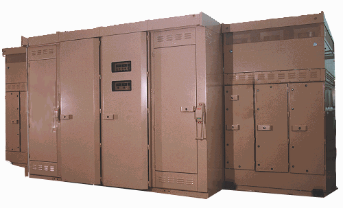
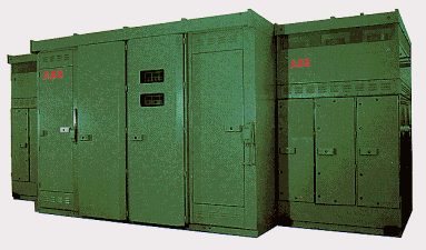
Figure 5, Pad Mount STS
Main Circuit Design
The main circuit of the STS comprises the
power electronic switches themselves, as well as the supporting breakers, and
isolation switches, and arrestor type over-voltage surge protection. The
arrangement of the supporting breakers, and interrupters is application
dependent, and may require a complete set of bypass and protective breakers, as
well as isolators to allow maintenance on portions of the switch, while other
components are live. It is also important that the switch, breakers and
isolators be easily integrated into exiting equipment line-ups including the
required cooling facilities as well as supporting the facility for outdoor
application such as dead-front pad-mounting. Figure 5 shows a view a pad mount
STS application for operation adjacent to a 69 kV substation feeding several
12.6 kV circuits. This outdoor application has facilities for complete bypass,
isolation, and breaker protection in standard size 15 kV switch-gear line-up
equipment. There is nothing very special about this arrangement, other than the
provision of PT, CT and CPT equipment to make the STS completely self
contained. Other than communication signals, the STS is completely self
contained, obtaining power directly from its 15 kV sources for operation of all
controls. The CPT power is redundant and obtained from each source with
provision to transfer control power on loss of feeder voltage.
The power electronic components are of
very special design. The switch design must be carefully considered in order to
meet the voltages that will be applied both from internal and external effects
of operation, and for normal as well as abnormal service. The current rating of
the switch together with the design of the snubber, defines the voltage
environment for the switch for internal effects. It is essential that the
switch be designed to meet the worst case voltage resulting from such service.
Normally, when either switch is properly conducting, and carrying up to rated
current (with no delay in firing), the switch voltage drop should be purely the
sum of diode drops associated with the number of thyristor elements in series;
essentially one volt per diode drop. This is true even on the non-conducting
switch if the phase angle between the sources is small. On switch blocking,
from an initial conducting state, the current in the switch will attempt to
continue to flow as the current in a circuit cannot be interrupted
instantaneously. Also the thyristor cannot establish a blocking state without
the flow of reverse recovery current. The transient process of reaching a
blocking state requires the switch to go from essentially zero voltage up-to
rated voltage with essentially equal division between levels. The peak voltage
reached in this process leads to transient over-voltage before returning to a
fully blocking state. The maximum voltage on each level is controlled by the
snubber design and the number of thyristor in series, and by the effect of any
varister elements that might be in parallel with each level or in parallel with
the switch.
The worst case external event of
over-voltage of an RLC circuit is typically twice rated voltage for a single
event. This situation is also true of the STS, except for special circumstances
such as ferro-resonance which may occur because of the effect of PT and CPT
magnetizing reactance and saturation, and snubber capacitive reactance.
Ferro-resonance of this kind may result when the switch is unloaded, such as a
line-drop on the alternate source, with the snubber and PT being driven from
the voltage of the preferred source. A more typical situation will be a line
down on the preferred source, causing transfer due to low voltage, resulting in
resonance driven from the alternate source. While over-voltage from this source
cannot be totally avoided, the persistent effect of resonant over-voltage can
be avoided by choosing the PT design carefully. Standard rated CT and PT
arrangements cannot generally be used in this application because of this fact.
STS Operation
This STS is connected to two 12.6 kV
feeders fed from a common 69 kV bus via two 69/12.6 kV transformers. The load
side of the STS is fed through a 12.6 kV to 480 volt Y/Y transformer to two 500
kW load banks in parallel, each switched in 25 kW increments. The 12.6 kV side
is also connected to a utility load in parallel with the load bank transformer.
During initial commissioning, this arrangement provided the means to transfer
to the utility load with current already flowing in the switch. This expedient
allows the load bank to be removed incrementally to be sure that there are no
start-up disturbances in this environment when there are only manually operated
by-pass switches available.
The switch has operated down to 8 amperes
load current, with more than adequate signal to noise in the control input
signals for current tracking firing control purposes, and has been transferred
manually and automatically many times.
The operation of the switch, to
demonstrate automatic transfers has been affected so far by the expedient of
removing a voltage signal from the operating side of the switch, to induce the
control into thinking an actual low-voltage condition exists on this phase. The
switch is then called to perform a transfer operation. Because there is no
actual low voltage condition, the transfer proceeds in the fashion of
break-before-make.
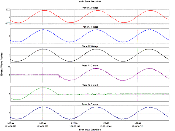
Figure
6, Automatic Transfer Test Operation
Figure 6, provides a plot taken from a
power quality meter of the sources and load phase ‘a’ voltages and currents
during a synthetic transfer event. The load voltage is taken from the low side
of the 12.6 kV/415 v transformer. It can be seen in this plot, there is a
slight delay in the start-up of the second source onto the load, following
current zero in the source going out. This delay can be minimized, but is
required, to properly distinguish the transfer point when it is initiated close
to a current zero, and especially when there is a phase angle difference
between source voltages.
The performance of the STS for loss of
voltage is demonstrated in the plot of Figure 7, for down-stream three-phase
bus voltage and phase ‘a’ current. Here the preferred source was tripped by
opening an 12.6 kV oil circuit breaker in the supply sub-station. The reduction
in voltage was sensed by the control which initiated the make-before-break
transfer sequence. The initiating event as seen by the PQ meter output, for the
protected downstream 125 volt circuit, is seen to be the reduction of the ‘b’
phase voltage. The event disturbance is seen to be very small and the complete
transfer, of all three phases, is over in about sixty degrees of the
fundamental wave-form, with essentially no disturbance in subsequent fundamental
wave-form. The harmonic content of the voltage wave-form immediately after
switching is a result of the lost volt-seconds (flux) in all of the down-stream
supply transformers, due to the voltage disturbance. Such voltage disturbance
after switching is normal and exists transiently until the transformer flux is
reestablished. The STS minimizes this effect by providing rapid transfer.
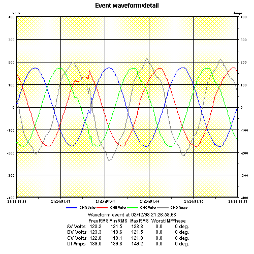
Figure
7, Automatic Transfer on loss of Preferred Source
Commissioning a complex electronic system
like the STS is a challenge because all of the sub-systems must be working
correctly at the point of full voltage application. Reduced voltage application
is not practical, and failure to work correctly due to misalignment of controls
can mean expensive component failures.
The first commissioning of the control
was performed in a novel manner that proved the functionality of all of the
controls and monitoring before the switch actually carried current. The method
was to apply the actual switch voltages and control power, but have the control
also use the voltage signals as a substitute for current signals. This
expedient allowed the control to think that it was in actual operation, and
allows the alignment of the firing pulses to current zero, the phase-out of the
switch, simulate transfer operation, and check for correct operation of all of
the monitoring for gate reception and temperature measurement, all before
seeing normal voltage for the first time. With this expedient, the first
operation was carried out without incident.
Conclusions
The STS is seen to be a relatively
complex device from a control and monitoring point-of-view. This complexity is
offset by the fact that there are many, many years of experience with thyristor
application where the reliability issues have needed to be addressed in order
to have a viable product, not-with-standing complexity and the large number of
components.
The main contribution in the STS, to
thyristor application technology, are the algorithms that make firing control
possible without delays at current zero crossings, and the near instantaneous
detection of fault direction to inhibit transfer of down stream faults. The
enabling technology for this is the modern floating point digital signal
processor, especially those that can be worked in parallel to share the volume
of calculations. The other valuable feature of the DSP is the ability to replace
much of the analog signal electronics of yesterday with digital computation.
This effect is a major help in increasing overall reliability of the
application by reducing the number of discrete components.
References
"Application Considerations for
Power Quality Equipment & Solutions for Distribution Networks", Colin
EJ Bowler, Vinod Bapat, Robert Hirt, Power Systems World 1997, Baltimore MD
September 6-12 1997.